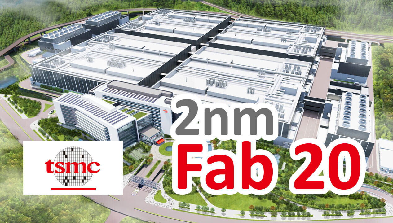
TSMC is moving quickly toward a major production milestone, aiming to bring four 2 nm fabs online by 2026, with a combined capacity of more than 60,000 wafers per month. In Kaohsiung's Nanzi park, TSMC has already started installing next-generation lithography scanners in Fab 22's new cleanroom. Its...


60,000 300 mm wafers would be enough for about 60 million Zen 5 CCDs per month assuming zero defects.
Realistically it would be even more since this is 2 nm we are talking about.
I was reading recently about how Nvidia gpu familes (i.e. the RTX 40xx series) all use the same architecture, but are separated by the number of defects on the board (as all nanofab-made electronics have a certain amount of defects). They are placed into different ‘bins’ that have certain ranges of defective components, but the functionality as a gpu is still fine. I imagine that other companies do this too, and with other electronics besides gpus. Also as mentioned in another comment, ‘2nm’ is a marketing term and does not indicate the actual size of the transistors. My point being: this may not result in larger supply of currently available electronics that use different architectures (4nm, 5nm process, etc). It is more likely to be a move to prepare facilities for next-gen electronics. I don’t know about specific companies intentions to move to ‘2nm’ processes for their products or how easy that actually is, though, so it would be a case by case check.
Yes, you are correct.
My comment was just a “back of the napkin” comment. At 2 nm (in the marketing sense), you would be able to make more AMD Zen 5 CCDs, but AMD wouldn’t even port Zen 5 to 2 nm, it would be Zen 6.
Now you’ve got me reading the wikipedia page on Zen 5 and 6 instead of working 👍
😆 Semiconductor can be fun. Nerdy, but fun!