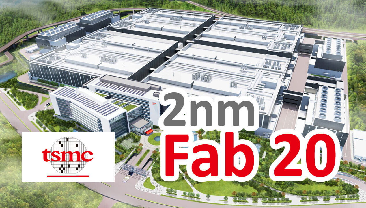
TSMC is moving quickly toward a major production milestone, aiming to bring four 2 nm fabs online by 2026, with a combined capacity of more than 60,000 wafers per month. In Kaohsiung's Nanzi park, TSMC has already started installing next-generation lithography scanners in Fab 22's new cleanroom. Its...


Yes, you are correct.
My comment was just a “back of the napkin” comment. At 2 nm (in the marketing sense), you would be able to make more AMD Zen 5 CCDs, but AMD wouldn’t even port Zen 5 to 2 nm, it would be Zen 6.
Now you’ve got me reading the wikipedia page on Zen 5 and 6 instead of working 👍
😆 Semiconductor can be fun. Nerdy, but fun!